|
|

The following appendix lists the pinouts for Ethernet, Token Ring, and synchronous serial appliques, and signal summaries for assorted cables.
Following is a list of the pinouts and signal summaries in this appendix:
By default, the console ports on the processor cards are wired for data communications equipment (DCE). Both DSR and DCD are active when your system is running. The RTS signal tracks the state of the CTS input. The console port does not support hardware flow control. The console port uses a female DB-25 connector. Table A-1 lists the DCE wiring scheme for the console port.
Table A-1 CPU Console Port RS-232 DCE Wiring Scheme
An auxiliary port is optionally supported for all processors. This is an asynchronous data terminal equipment (DTE) port on the processor card (CSC/3 and CSC/4) to which an RS-232 port from a CSU/DSU or protocol analyzer can be attached for access from the network.
The auxiliary port shares the ribbon cable between the processor card and the console port. The console-port end of the cable is split, so it has two DB-25 connectors at the connector-panel end: one for the console port and one for the auxiliary port. The processor-card end of the cable has one 50-pin ribbon connector, which connects to the console cable port on the processor card. The auxiliary port uses a male DB-25 connector. Table A-2 lists the signals used on this port.
Table A-2 CPU Auxiliary Port RS-232 DTE Wiring Scheme
|
| 1 Both DTR and RTS are active when your system is running. Modem-control signals are ignored. The auxiliary port does not support hardware flow control. |
To use the dial-on-demand feature (discussed in the configuration guide publication) with some synchronous modems, you might need special cable configurations. If your modem follows the
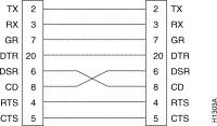
V.25 bis specification and raises Data Set Ready (DSR), a cable modification is required to swap DSR with Data Carrier Detect (DCD or CD). If your modem ignores the V.25 bis specification and raises DCD, no cable modifications are required. Figure A-1 shows the configuration for the RS-232 cable, and Figure A-2 shows the configuration for the HD V.35 cable.
For the RS-232 cables, swap pin 6 (DSR) with pin 8 (CD) at either end.
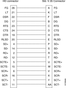
Receive Line Signal Detect (RLSD) is the HD V.35 equivalent of CD. For the high-density (HD) V.35 cables, swap pin E (DSR) with pin F (RLSD) at the standard V.35 end, or swap pin 20 (DSR) with pin 22 (RLSD) at the HD end. The results are shown in Figure A-2.
As you use your router, it may become necessary to modify, build, or repair cables, and this appendix provides the pinouts you will need. If an applique contains jumpers that allow any modifications of the applique, that information also is included.
The next three sections cover Ethernet and Token Ring appliques. The following appliques are included: Ethernet 10BaseT,Ethernet AUI, and Token Ring.
The Ethernet 10BaseT applique (see Figure A-3) combines an RJ-45 connector for direct connection to an unshielded twisted-pair (UTP) network segment and a UTP tranceiver. The 10BaseT applique is compliant with IEEE 802.3. The pinout for the 10BaseT RJ-45 connector is listed in Table A-3.
Table A-3 10BaseT RJ-45 Connector Pinout
An attachment unit interface (AUI) transceiver must be used with most Ethernet products. (The 10BaseT transceiver applique is an exception to this.) Transceivers are available from a variety of sources for AUI, thick LAN, thin LAN, twisted-pair Ethernet, and other media. Table A-4 lists the Ethernet AUI pinout.
Table A-4 Ethernet (AUI) Pinout
There are several types of twisted-pair cable. Unshielded twisted-pair (UTP) cable should be 26 to 22 American wire gauge (AWG)—0.4 to 0.6-millimeter (mm)—wire in a multiwire cable with
100-ohm impedance. The 802.3 specification states that the maximum length of a 10BaseT link segment is 100 meters or 328 feet of UTP wiring. Do not exceed these limits.
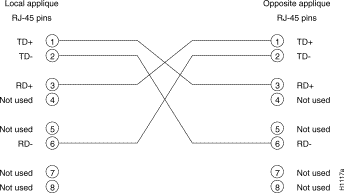
If you are not connected to a hub, and another 10BaseT transceiver applique is connected to the opposite end of your link, the UTP cabling must be crossed as shown in Figure A-4. The RD- and RD+ signals must be swapped with the TD- and TD+ signals. When the opposite end of your link is connected to a hub, the hub performs this crossover function, and it is not necessary to cross the cables.
The pinout for the Token Ring applique used with the CSC-1R, CSC-2R, and CSC-R16M cards is listed in Table A-5.
Table A-5 CSC-1R, CSC-2R, and CSC-R16M Token Ring Connector Pinout
Note The CPT chassis cannot use Token Ring
interfaces. The CGS chassis can use the CSC-2R card only. The MGS
chassis can use the CSC-1R, CSC-2R, and CSCR16M cards.
The following sections discuss the pinouts and jumpers for the following serial appliques and cables. In the serial applique pinout tables, the symbols <— and —> indicate signal direction with respect to DCE and DTE devices. For example, "DCE <— DTE" means this signal is from DTE to DCE.
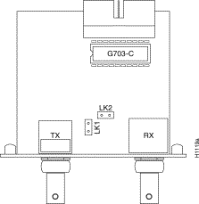
The G.703 network interface is the output port, consisting of two BNC connectors (TX and RX), adjacent to the approval symbol. The input port is connected by a ribbon cable to either a CSC-MCI or CSC-SCI interface card. Clocking (timing) for the G.703 applique is derived from the network input at approximately 2048 kilobits per second (Kbps) (E1 speed). The G.703 supports only DTE. You must use two 75-ohm coaxial cables, of diameter 5 mm, terminated in male BNC connectors with maximum cable attenuation of 6 decibels (dB) at 1024 kilohertz (KHz). Attenuation characteristics should follow the root f law. The outer conductor is isolated from system earth. A single applique can be mounted on an individual plate. Figure A-5 shows the layout of the G.703 applique.
These warning notices apply to the Input Port, the port marked "SAFETY WARNING: see instructions for use."
Interconnection of the applique input port (the port marked "SAFETY WARNING: see instructions for use"), directly, or by way of any other apparatus, with ports on other apparatus (marked or not so marked) may produce hazardous conditions on the network. Users should seek advice from a competent engineer before making such a connection. The applique is approved as Independent of Host. As such, the applique is only approved for use with a host and with host attachments that are either type approved in their own right, or, if supplied after 1st March 1989, are covered by the terms of the General Approval number NS/G/1234/J/100003. A Host supplied under the terms of the General Approval number NS/G/1234/J/100003 satisfies the conditions of the paragraphs above. The applique must not be modified in any way. Any form of modification invalidates the approval for connection and the warranty of the unit. The applique approval label must be visible externally. The approval label must not be detached from the applique, nor attached to the host. The terms of the approval require that there must be a minimum distance (5 mm) between the applique and any other part of the host, including other appliques. This condition is met by default when the applique is installed in a chassis enclosure in accordance with the instructions. If voltages greater than 250V are present in the host, users should refer to a competent safety engineer for advice. It is a condition of the approval that a copy of these user instructions and safety warnings must be supplied with the host. Failure to provide the applique user instructions with the host will invalidate the applique approval. Failure to install the applique in accordance with these instructions will invalidate the approval. If you experience difficulties, or are in any doubt, contact a customer service representative.
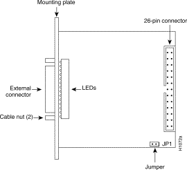
The high-density (HD) V.35 applique carries the same signals as the old-style V.35 applique, but provides them on a smaller 26-pin HD connector (the old-style applique used a 38-pin connector). The smaller 26-pin connector is male on all four versions of the HD V.35 cable, and the larger 34-pin connector on each cable carries the male or female configuration. The cable used determines the mode of the applique. Table A-6 lists the pinout for the HD V.35 applique (and cable) when used as a DCE or DTE interface. The HD V.35 applique and external interface cable options are listed by product number in Table A-7 and Table A-8, respectively.
Table A-6 HD V.35 Dual-Mode Applique and Cable Pinout
91
Table A-7 HD V.35 Appliques by Product Number
Table A-8 lists the four external interface cables available for the HD V.35 applique and provides the product numbers. The HD V.35 supports both DTE and DCE modes; the external HD V.35 cable attached to the applique determines this mode. The cable has a 26-pin male connector on one end and a 34-pin male or female connector on the other end.
Table A-8 HD V.35 External Interface Cables by Product Number
The HD V.35 applique has only one jumper (JP1), which selects Serial Clock Transmit (SCT) (to the DTE) or Serial Clock Transmit External (SCTE) (from the DTE) as the timing source for Signal Detect (SD) when the applique is in DCE mode. The default is SCTE (for DTE), which is selected when the JP1 jumper is in. To select SCT (for DCE), remove the jumper. The cable used determines the mode of the applique. The HD V.35 applique is illustrated in Figure A-6.
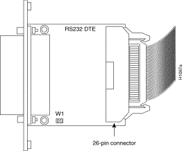
The RS-232 DCE and DTE appliques have either a female (for DCE) or male (for DTE) 25-pin D-type connector. The mode is fixed for each applique and printed on the applique. (See the DTE applique in Figure A-7.) The internal ribbon cable attaches to the 26-pin connector. Table A-9 lists the pinouts for the RS-232 DCE and DTE appliques.
Table A-9 RS-232 DCE and DTE Applique Pinouts
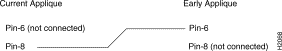
Very early MCI cards were shipped with an RS-232 DTE applique assembly designed by a third-party vendor. These older appliques, marked SCO-232, do not have any LEDs. If you are using this RS-232 DTE applique assembly on the other side of a link, the applique has Carrier Detect (CD) on pin 6, which is contrary to current RS-232 specifications. When using this applique with an RS-232 DCE applique assembly, you must use a cable adapter or breakout box to change the cable as shown in Figure A-8. All other signals on the 25-pin cable should be straight through.
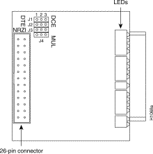
The Synchronous Data Link Control (SDLC) nonreturn to zero inverted (NRZI) applique has a female 25-pin D-type connector. An internal ribbon cable attaches to the 26-pin connector. (See Figure A-9.) Jumpers J1 and J2 set the mode (DCE or DTE); J3 sets the nonreturn to zero function; and J4 has no user function (default position on pin 1 and 2). (See Table A-10.) Table A-11 lists the pinout for the SDLC DCE applique and the crossover cable required when the SDLC applique is used in DTE mode.
Table A-10 RS-232 SDLC Applique Jumpers
DTE1
Defautlt2
2 Leave J4 in the default position.
Table A-11 Pinout for the SDLC DCE Applique and the Crossover Cable
NC1
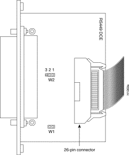
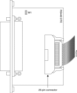
The RS-449 DTE applique contains a male 37-pin connector, while the RS-449 DCE applique contains a female 37-pin connector. The internal ribbon cable connects to the 26-pin connector. The mode is labeled on the circuit card (either RS-449 DTE or RS-449 DCE). The RS-449 DCE applique is shown in Figure A-10, and the RS-449 DTE is shown in Figure A-11.
The RS-449 DCE applique requires that the clocking be supplied from the MCI card or the SCI card. The DCE applique contains an additional jumper field (W2) which selects the transmit data clock source. Pins 1 and 2 of W2 are jumpered together causing the applique to expect to see the transmit clock on the serial clock transmit external (SCTE/TT) lines of the interface cable.
It is important that the DTE attached to this interface returns SCTE/TT along with its data to avoid cable-induced clocking problems. This is the factory default, and it is the recommended setting for reliable operation at high data rates. If the DTE device does not return a clock on SCTE/TT, connecting pins 2 and 3 of W2 together causes the DCE applique to use the outgoing clock serial clock transmit (SCT/ST) instead of SCTE/TT.
The RS-449 DTE applique (see Figure A-11) returns transmit clock on SCTE/TT. This is designed to compensate for clock phase shifting on long cables. It is important that the DCE device connected to the DCE applique modem be configured to accept SCTE/TT.
On both the DTE and DCE RS-449 appliques, pin 10 carries the local loopback (LL) signal. Use the software configuration subcommand loopback to invoke loopback to check out your installation or to verify that the applique is functioning correctly. The loopback command will assert pin 10 (LL) in DTE mode and will loop the Send Data (SDA and SDB) signals to the Receive Data (RDA and RD) signals. If the DCE applique ever gets the loopback pin (pin 11) asserted by the DTE device, it will loop SDA and SDB to RDA and RDB.
Following is sample output of the loopback command for serial 0:
The no loopback command returns the interface to normal function.
Table A-12 lists the pinouts for the RS-449 DCE and DTE appliques.
Table A-12 RS-449 DCE and DTE Applique Pinout
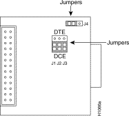
The X.21 applique, which is designed for domestic and international use, meets the CCITT specification for a DTE, VDE Class B, and FCC Class A, CSA C108.8. The applique can be set for either DTE or DCE mode, with default mode as DTE. Change the mode to DCE by changing the position of jumpers J1, J2, and J3. (See Figure A-12.) All three jumpers must be in the same position (DCE or DTE) in order for the applique to operate properly. Jumper J4 connects logic ground to chassis ground when in the default position. (See Figure A-12.) Special DTE and DCE cables are required for DTE or DCE operation. Table A-13 lists the pinout for the X.21 applique.
Table A-13 X.21 Applique Pinouts
DCE Clock - a1
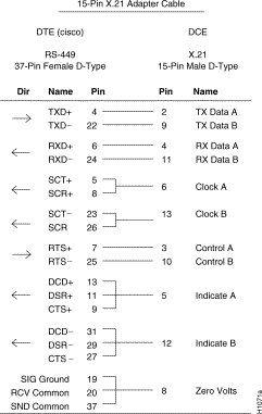
Figure A-13 provides the pinout for constructing an X.21 to RS-449 transition cable. This is of particular importance for X.21 connections in the United Kingdom and Germany.
Serial Applique Pinouts
or data terminal equipment (DTE), page 9 G.703 Applique
Figure A-5 G.703 Applique—Component-Side View
Safety Warnings and Requirements for the G.703
![]()
Warning
![]()
Warning
![]()
Warning
![]()
Warning
HD V.35 Dual-Mode Applique
Applique/Cable
(26-Pin Connector)
Cable
(34-Pin Connector)
Pins
Direction
DCE DTE
Pins
Pins
Mnemonic
Function
1 Pins 9 and 18 are tied together to force the applique to be DCE when the DTE/DCE jumper on the MCI or SCI card is set for DCE, and the appropriate cable is used.
Product No.
Mode1
Plate Size
Number of Interfaces
1 If an individual DTE HD V.35 applique is ordered, the product number APP-IX1 is used (X = HD V.35). The mode of the applique must be indicated as DTE or DCE so that the appropriate cable can accompany the applique. If an individual applique without a mounting plate is required, use APP-X=.
HD V.35 Cables
Product No.
Mode1
Cable Gender
(26 pin to 34 pin)
1 Each applique is shipped with the appropriate interface cable depending on the mode of the applique (DTE or DCE) and the cable gender required.
Figure A-6 HD V.35 Applique—Bottom View
RS-232 DCE and DTE Appliques
Figure A-7 RS-232 DTE Applique—Component-Side View
Older RS-232 Appliques
Figure A-8 Cable Change Required When Using Older RS-232 Applique
RS-232 SDLC Dual-Mode Applique
Figure A-9 SDLC Applique—Component-Side View
Jumper Pin Numbers
Jumper
1
2
3
Function
1 Using the SDLC applique for DTE requires a crossover cable that grounds pin 11 of the applique for DTE selection. (See Table A-11.)
SDLC DCE Applique and Router End
of the Crossover Cable (DTE)
Network End
of the Crossover Cable (DCE)
DB-25 Male
DB-25 Female
Mnemonic
Pin
Mnemonic
Pin
1 NC = No connection; however, using the SDLC applique for DTE mode requires the CAB-R32NZ crossover cable that ties pin 11 to ground for DTE selection. The part number for this crossover cable is 72-0757-01.
RS-449 DCE and DTE Appliques
Figure A-10 RS-449 DCE Applique—Component-Side View
Figure A-11 RS-449 DTE Applique—Component-Side View
X.21 Dual-Mode Applique
Figure A-12 X.21 Applique with Jumpers Set for DCE Operation—Component-Side View
Pin
DTE Mnemonic/Function
Direction
DTE DCE
Pin
DCE Mnemonic/Function
1 These signals go to the DCE device only when the jumpers are set for DCE, and the DCE transition cable is used.
X.21 to RS-449 Adapter Cable
Figure A-13 15-Pin X.21 to RS-449 Adapter Cable Pinout
![]()
![]()
![]()
![]()
![]()
![]()
![]()
![]()
Posted: Thu Nov 6 15:53:57 PST 2003
All contents are Copyright © 1992--2003 Cisco Systems, Inc. All rights reserved.
Important Notices and Privacy Statement.